- 您现在的位置:买卖IC网 > Sheet目录513 > SI7461DP-T1-GE3 (Vishay Siliconix)MOSFET P-CH 60V 8.6A PPAK 8SOIC
�� �
�
�Si7461DP�
�www.vishay.com�
�P-Channel� 60� V� (D-S)� MOSFET�
�Vishay� Siliconix�
�PRODUCT� SUMMARY�
�V� DS� (V)� R� DS(on)� (� ?� )�
�0.0145� at� V� GS� =� -10� V�
�-60�
�0.019� at� V� GS� =� -4.5� V�
�I� D� (A)�
�-14.4�
�-12.6�
�FEATURES�
�?� TrenchFET� ?� Power� MOSFETs�
�?� Low� thermal� resistance� PowerPAK� ?� package�
�with� low� 1.07� mm� profile�
�?� Material� categorization:�
�For� definitions� of� compliance� please� see�
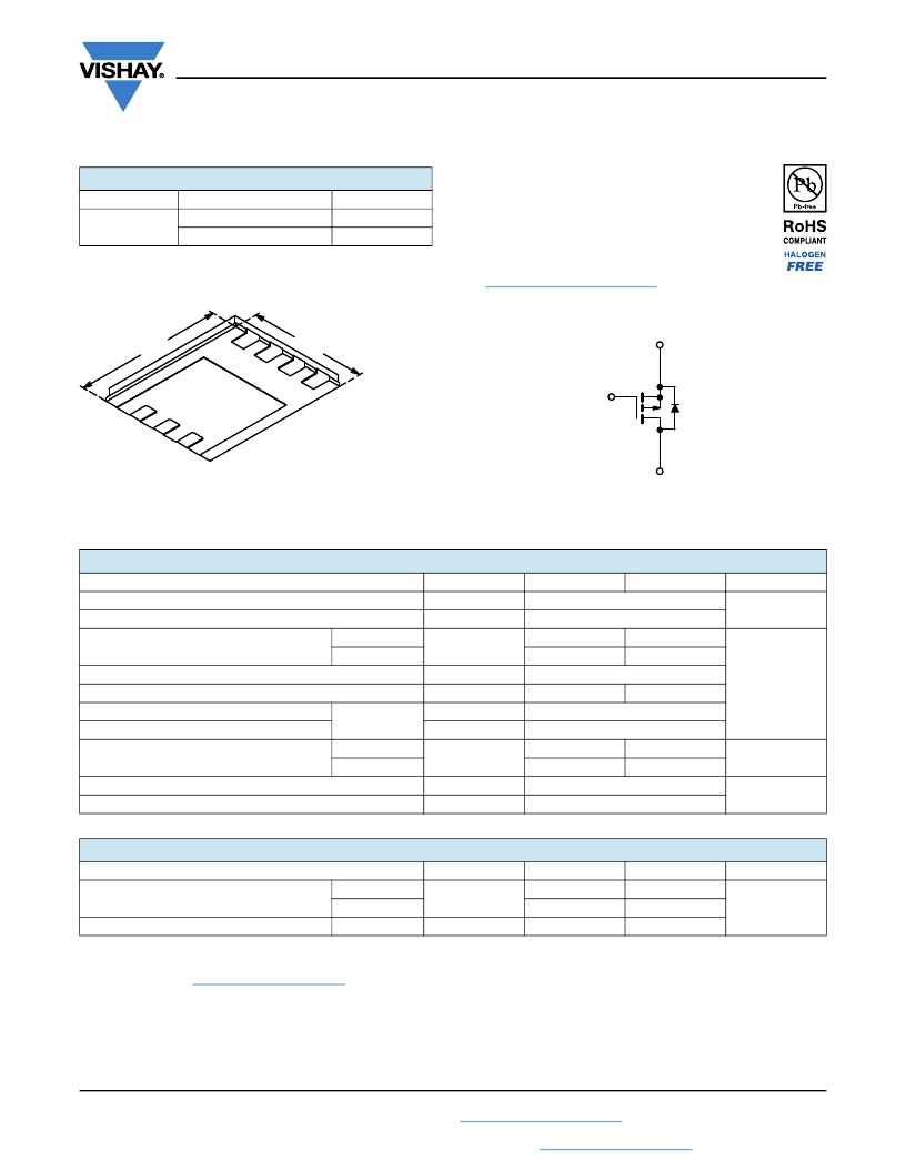
�PowerPAK� SO-8�
�www.vishay.com/doc?99912�
�S�
�Availa� b� le�
�6.15� mm�
�1�
�S�
�S�
�5.15� mm�
�2�
�3�
�S�
�G�
�D�
�4�
�G�
�8�
�7�
�D�
�D�
�6�
�5�
�D�
�Bottom� View�
�Ordering� Information:� Si7461DP-T1-E3� (Lead� (Pb)-free)�
�Si7461DP-T1-GE3� (Lead� (Pb)-free� and� Halogen-free)�
�ABSOLUTE MAXIMUM RATINGS� (T� A� = 25 °C, unless otherwis� e� noted)�
�D�
�P-Channel� MOSFET�
�PARAMETER�
�Drain-Source� Voltage�
�Gate-Source� Voltage�
�SYMBOL�
�V� DS�
�V� GS�
�10� s�
�STEADY� STATE�
�-60�
�±� 20�
�UNIT�
�V�
�Continuous� Drain� Current� (T� J� =� 150� °C)� a�
�T� A� =� 25� °C�
�T� A� =� 70� °C�
�I� D�
�-14.4�
�-11.5�
�-8.6�
�-6.9�
�Pulsed� Drain� Current�
�Continuous� Source� Current� (Diode� Conduction)� a�
�Avalanche� Current�
�Single� Pulse� Avalanche� Energy�
�L� =� 1� mH�
�I� DM�
�I� S�
�I� AS�
�E� AS�
�-4.5�
�-60�
�50�
�125�
�-1.6�
�A�
�Maximum� Power� Dissipation� a�
�T� A� =� 25� °C�
�T� A� =� 70� °C�
�P� D�
�5.4�
�3.4�
�1.9�
�1.2�
�W�
�Operating� Junction� and� Storage� Temperature� Range�
�Soldering� Recommendations� (Peak� Temperature)� b,� c�
�T� J� ,� T� stg�
�-55� to� 150�
�260�
�°C�
�THERMAL� RESISTANCE� RATINGS�
�PARAMETER�
�SYMBOL�
�TYPICAL�
�MAXIMUM�
�UNIT�
�Maximum� Junction-to-Ambient� a�
�Maximum� Junction-to-Case� (Drain)�
�t� ?� 10� s�
�Steady� State�
�Steady� State�
�R� thJA�
�R� thJC�
�18�
�52�
�1�
�23�
�65�
�1.3�
�°C/W�
�Notes�
�a.� Surface� mounted� on� 1"� x� 1"� FR4� board.�
�b.� See� solder� profile� (� www.vishay.com/ppg?73257� ).� The� PowerPAK� SO-8� is� a� leadless� package.� The� end� of� the� lead� terminal� is� exposed� copper�
�(not� plated)� as� a� result� of� the� singulation� process� in� manufacturing.� A� solder� fillet� at� the� exposed� copper� tip� cannot� be� guaranteed� and� is� not�
�required� to� ensure� adequate� bottom� side� solder� interconnection.�
�c.� Rework� conditions:� manual� soldering� with� a� soldering� iron� is� not� recommended� for� leadless� components.�
�S13-2282-Rev.� H,� 04-Nov-13�
�1�
�Document� Number:� 72567�
�For� technical� questions,� contact:� pmostechsupport@vishay.com�
�THIS� DOCUMENT� IS� SUBJECT� TO� CHANGE� WITHOUT� NOTICE.� THE� PRODUCTS� DESCRIBED� HEREIN� AND� THIS� DOCUMENT�
�ARE� SUBJECT� TO� SPECIFIC� DISCLAIMERS,� SET� FORTH� AT� www.vishay.com/doc?91000�
�发布紧急采购,3分钟左右您将得到回复。
相关PDF资料
SI7462DP-T1-GE3
MOSFET N-CH D-S 200V 8-SOIC
SI7465DP-T1-GE3
MOSFET P-CH 60V 3.2A PPAK 8SOIC
SI7530DP-T1-GE3
MOSFET N/P-CH 60V PWRPAK 8-SOIC
SI7620DN-T1-GE3
MOSFET N-CH 150V 13A 1212-8
SI7625DN-T1-GE3
MOSFET P-CH D-S 30V 1212-8 PPAK
SI7629DN-T1-GE3
MOSFET P-CH 20V 1212-8 PPAK
SI7634BDP-T1-E3
MOSFET N-CH D-S 30V PPAK 8SOIC
SI7636DP-T1-GE3
MOSFET N-CH D-S 30V PPAK 8SOIC
相关代理商/技术参数
SI7462DP
制造商:VISHAY 制造商全称:Vishay Siliconix 功能描述:N-Channel 200-V (D-S) MOSFET
SI7462DP-T1-E3
功能描述:MOSFET 200V 4.1A 4.8W 130mohm @ 10V RoHS:否 制造商:STMicroelectronics 晶体管极性:N-Channel 汲极/源极击穿电压:650 V 闸/源击穿电压:25 V 漏极连续电流:130 A 电阻汲极/源极 RDS(导通):0.014 Ohms 配置:Single 最大工作温度: 安装风格:Through Hole 封装 / 箱体:Max247 封装:Tube
SI7462DP-T1-GE3
功能描述:MOSFET 200V 4.1A 4.8W 130mohm @ 10V RoHS:否 制造商:STMicroelectronics 晶体管极性:N-Channel 汲极/源极击穿电压:650 V 闸/源击穿电压:25 V 漏极连续电流:130 A 电阻汲极/源极 RDS(导通):0.014 Ohms 配置:Single 最大工作温度: 安装风格:Through Hole 封装 / 箱体:Max247 封装:Tube
SI7463ADP-T1-GE3
制造商:Vishay Semiconductors 功能描述:MOSFETS - Tape and Reel 制造商:Vishay Intertechnologies 功能描述: 制造商:Vishay Siliconix 功能描述:FET P-CH 40V 16.6A PPAK 8SOIC 制造商:Vishay Intertechnologies 功能描述:DUAL P-CHANNEL 20-V (D-S) MOSFET 制造商:Vishay Intertechnologies 功能描述:MOSFET
SI7463DP
制造商:Vishay Siliconix 功能描述:MOSFET P POWERPAK
SI7463DP-T1
制造商:Vishay Siliconix 功能描述:TRANS MOSFET P-CH 40V 11A 8PIN PWRPAK SO - Tape and Reel
SI7463DP-T1-E3
功能描述:MOSFET 40V 18.6A 5.4W 9.2mohm @ 10V RoHS:否 制造商:STMicroelectronics 晶体管极性:N-Channel 汲极/源极击穿电压:650 V 闸/源击穿电压:25 V 漏极连续电流:130 A 电阻汲极/源极 RDS(导通):0.014 Ohms 配置:Single 最大工作温度: 安装风格:Through Hole 封装 / 箱体:Max247 封装:Tube
SI7463DP-T1-GE3
功能描述:MOSFET 40V 18.6A 5.4W 9.2mohm @ 10V RoHS:否 制造商:STMicroelectronics 晶体管极性:N-Channel 汲极/源极击穿电压:650 V 闸/源击穿电压:25 V 漏极连续电流:130 A 电阻汲极/源极 RDS(导通):0.014 Ohms 配置:Single 最大工作温度: 安装风格:Through Hole 封装 / 箱体:Max247 封装:Tube